- 您现在的位置:买卖IC网 > Sheet目录2007 > MAX1011CEG+ (Maxim Integrated Products)IC ADC 6BIT 90MSPS 24-QSOP
MAX1011
Low-Power, 90Msps, 6-Bit ADC
_______________________________________________________________________________________
3
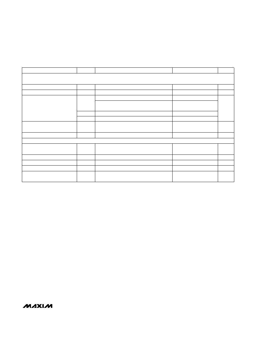
AC ELECTRICAL CHARACTERISTICS
(VCC = +5V ±5%, VCCO = 3.3V ±300mV, TA = +25°C, unless otherwise noted.)
Note 1: Best-fit straight-line linearity method.
Note 2: A typical application will AC couple the analog input to the DC bias level present at the analog inputs (typically 2.35V).
However, it is also possible to DC couple the analog input (using differential or single-ended drive) within this common-
mode input range (Figures 4 and 5).
Note 3: PSRR is defined as the change in the mid-gain, full-scale range as a function of the variation in VCC supply voltage,
expressed in decibels.
Note 4: The current in the VCCO supply is a strong function of the capacitive loading on the digital outputs. To minimize supply tran-
sients and achieve optimal dynamic performance, reduce the capacitive-loading effects by keeping line lengths on the dig-
ital outputs to a minimum.
Note 5: Offset-correction compensation enabled, 0.22F at compensation inputs (Figures 2 and 3).
Note 6: tPD and tSKEW are measured from the 1.4V level of the output clock, to the 1.4V level of either the rising or falling edge of a
data bit. tDCLK is measured from the 50% level of the clock-overdrive signal on TNK+ to the 1.4V level of DCLK. The capac-
itive load on the outputs is 15pF.
GAIN = GND, open, VCC
GAIN = open (mid gain), fIN = 50MHz,
-1dB below full scale
GAIN = open (mid gain)
5.7
ENOBM
5.6
5.85
Effective Number of Bits
GAIN = open (mid gain)
GAIN = GND (low gain)
Guaranteed by design
CONDITIONS
MHz
55
BW
Analog Input -0.5dB Bandwidth
Msps
90
fMAX
Maximum Sample Rate
GAIN = VCC (high gain)
LSB
OFF
Input Offset (Note 5)
-0.5
0.5
dB
35.5
37
SINAD
Signal-to-Noise Plus Distortion
Ratio
Bits
5.85
ENOBL
5.8
ENOBH
(Note 6)
ns
1
tSKEW
Data Valid Skew
ns
3.0
tPD
Clock to Data Propagation
Delay
UNITS
MIN
TYP
MAX
SYMBOL
PARAMETER
TNK+ to DCLK (Note 6)
ns
4.5
tDCLK
Input to DCLK Delay
Figure 8
ns
5.5
tAD
Aperture Delay
Figure 8
clock
cycle
1
PD
Pipeline Delay
TIMING CHARACTERISTICS (Data outputs: RL = 1M, CL = 15pF)
DYNAMIC PERFORMANCE (Gain = open, external 90MHz clock (Figure 7), VIN = 20MHz sine, amplitude -1dB below
full scale, unless otherwise noted.)
发布紧急采购,3分钟左右您将得到回复。
相关PDF资料
MAX105ECS+T
IC ADC 6BIT 800MSPS DL 80TQFP
MAX1063AEEG+
IC ADC 10BIT 250KSPS 24-QSOP
MAX107ECS+
IC ADC 6BIT 400MSPS DL 80-TQFP
MAX1080AEUP+
IC ADC 10BIT 400KSPS 20-TSSOP
MAX1084AESA+
IC ADC 10BIT 400KSPS 8-SOIC
MAX1093AEEG+
IC ADC 10BIT 250KSPS 24-QSOP
MAX1098CEAE+
IC ADC 10BIT SERIAL 16-SSOP
MAX11040GUU+T
IC ADC 24BIT 4CH 38-TSSOP
相关代理商/技术参数
MAX1011CEG+T
功能描述:模数转换器 - ADC Low-Power 90Msps 6-Bit RoHS:否 制造商:Texas Instruments 通道数量:2 结构:Sigma-Delta 转换速率:125 SPs to 8 KSPs 分辨率:24 bit 输入类型:Differential 信噪比:107 dB 接口类型:SPI 工作电源电压:1.7 V to 3.6 V, 2.7 V to 5.25 V 最大工作温度:+ 85 C 安装风格:SMD/SMT 封装 / 箱体:VQFN-32
MAX1011CEG-T
功能描述:模数转换器 - ADC RoHS:否 制造商:Texas Instruments 通道数量:2 结构:Sigma-Delta 转换速率:125 SPs to 8 KSPs 分辨率:24 bit 输入类型:Differential 信噪比:107 dB 接口类型:SPI 工作电源电压:1.7 V to 3.6 V, 2.7 V to 5.25 V 最大工作温度:+ 85 C 安装风格:SMD/SMT 封装 / 箱体:VQFN-32
MAX1011EVKIT
功能描述:数据转换 IC 开发工具 RoHS:否 制造商:Texas Instruments 产品:Demonstration Kits 类型:ADC 工具用于评估:ADS130E08 接口类型:SPI 工作电源电压:- 6 V to + 6 V
MAX101A
制造商:MAXIM 制造商全称:Maxim Integrated Products 功能描述:500Msps, 8-Bit ADC with Track/Hold
MAX101ACFR
制造商:Maxim Integrated Products 功能描述:- Rail/Tube
MAX101ACFR1
制造商:Maxim Integrated Products 功能描述:84 PINS CERFP PKG - Bulk
MAX101ACFR-W
制造商:Maxim Integrated Products 功能描述:84 PINS CERFP PKG - Bulk
MAX101AEVKIT
制造商:Maxim Integrated Products 功能描述:KIT PKG - Bulk